Digital Protocols: How does JTAG work?
- Elias Themeßl

- 12. Feb.
- 4 Min. Lesezeit
JTAG stands for Joint Test Action Group and it is a hardware debugging interface. It was developed to standardize and simplify the testing and debugging of ICs.
As the development of printed circuit boards progressed in the 1980s and the use of multilayer printed circuit boards became more common, it became increasingly important to have simple and cost-effective ways to test the hardware.
JTAG is very powerful. With the so-called boundary scan of JTAG, it is possible to control individual pins of the respective ICs and set them to high or low. Thus, each individual component on a printed circuit board can be tested in great detail.
To perform such a boundary scan, it is necessary to have the BSDL file. BSDL stands for Boundary Scan Description Language. It is a file that contains all the information about the chip used. BSDL is a derivative of VHDL (Virtual Hardware Description Language), a software that hardware designers like to use to virtually build digital circuits using software.
It can be challenging to find such BSDL files. One simply has to search online for suitable matches. With some luck, this is possible, but the process can be very time-consuming.
JTAG is more suitable for testing a board as a whole. It is less suitable for controlling and testing individual chips.
With the use of JTAG, it is even possible to control other protocols used. Since the pins, for example I2C can be operated, it is possible to use JTAG to send signals that control other chips. Of course, this also applies to all other protocols supported by the chip.
Very well-known software that is also free includes UrJtag or JTAG Boundary Scanner. Both software packages are open source and are perfect for beginners. Of course, there is other software that is available for purchase or has a subscription model. TopJTAG is worth mentioning here.
JTAG usually has 4, 5, or sometimes 6 pins:
TDI - Test Data In - Data is sent to the chip at this pin.
Each manufacturer is responsible for developing the respective protocol. There is no uniform standard for the type of data transmission.
TDI - Test Date In - Data is sent to the chip. Every developer is responible for the protocol that they use. There is no common standard for it.
TDO - Test Data Out - Data is sent from the chip at this pin.
TCK - Test Clock - TCK is responsible for the clock speed. (This is also not defined in the protocol and is specified by the JTAG test device.)
TMS - Test Mode Select - The transmission is checked at this pin. The voltage at the TMS pin is measured at each clock. If the voltage falls below a certain level, it is interpreted as logical 0. If the voltage remains above a defined level, the state is considered logical 1.
TRST - Test Reset - The part of the circuit to be tested is reset.
SRST - System Reset - The entire system is reset.
The first 4 pins are usually always present when JTAG is available. The last two, TRST and SRST, are optional. TRST resets the test environment, SRST resets the entire system.
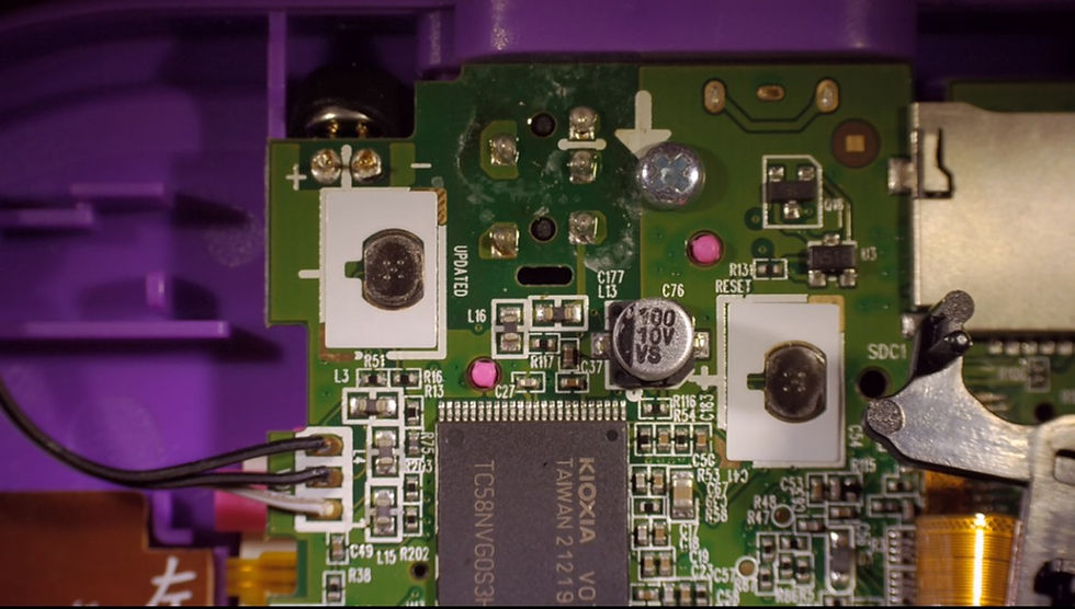
A disadvantage of JTAG is that the headers on the board are not always labeled. Thus, the pins for JTAG often have to be determined experimentally.
A tool called JTAGULATOR, developed by Joe Grand, can help with this. It automatically finds the correct JTAG pins, but to be honest, if you know what you´re doing, you absolutely don´t need that specific device which meanwhile isn´t in production anymore, if I´m not wrong.
With a lot of patience and careful experimentation, the pins can also be found manually. For beginners, I recommend starting with simple means and gradually moving on to more advanced tools. However, this is always a question of price.
Of course, hardware manufacturers often do not want others to disassemble their devices for reverse engineering purposes and explore how the technology works. For this reason, JTAG can often be made inaccessible in various ways. Besides the fact that JTAG headers may not be labeled, it can also happen that the pins are simply not present on the board. In this case, the contacts must be soldered manually to the pins of the chip, provided the chip has JTAG.
In some cases, so-called OTP fuses may be used. These are "fuses" that are present in the chip itself. After the board has been tested after production, these OTPs are triggered. Further use of the JTAG headers is thus impossible.
Another way manufacturers make access to JTAG more difficult is by using cryptographic keys.
In this case you would have to use advanced techniques such as fault injection or side-channel attacks which can be very time consuming. These two techniques maybe will be described in more detail in the future here.
To communicate with JTAG interfaces, a special hardware adapter is required. The Segger J-Link is just one example.
However, there are countless cheaper alternatives available online if you search for them such as this clone from china.

OpenOCD can also be recommended as software.
In conclusion, access to JTAG is not necessarily required. In theory, every function possible with JTAG can also be performed manually. It is just much easier to use JTAG. Thus, it is not directly a security vulnerability if JTAG is not disabled during production.


Comments